- September 11, 2025
- News
Summary
The sheer scale of the global chip market means that any manufacturing defect can have a costly ripple effect.

GILCHING, Germany, Sept. 11, 2025 – Optical inspection systems used in semiconductor fabrication must be capable of identifying both surface and subsurface flaws in wafers, ingots and semiconductor die. If not detected, these flaws can severely degrade the electrical properties, structural integrity, and downstream performance of the packaged chip.
Short Wavelength Infra-Red (SWIR) cameras are particularly well-suited for this task. Silicon is transparent to SWIR wavelengths, typically around 1,100 nm, allowing visualization of internal structures and subsurface defects like micro-cracks, impurities or particles that are invisible with visible light and standard machine vision cameras.
Foundation of modern electronics
The basic building blocks of virtually all electronic devices, from PCs and smartphones to cars, medical devices and industrial robotics, are integrated circuits or chips, which are made from processed silicon wafers. Soaring demand for advanced chips for artificial intelligence (AI) and high-performance computing is expected to push global semiconductor sales to a staggering $728 billion, according to World Semiconductor Trade Statistics.
The sheer scale of the global chip market means that any manufacturing defect can have a costly ripple effect, underscoring the importance of optical inspection in ensuring quality standards are met.
SVS-Vistek SWIR Cameras
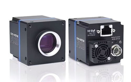
To help semiconductor foundries improve quality and yield, SVS-Vistek SenSWIR FXO cameras are available with resolutions up to 5.2 megapixels. SenSWIR FXO cameras have an extended wavelength range from 400 to 1700 nm that enables simultaneous recording of SWIR and visible images, eliminating the need for dual camera setups. High resolution is supported by 10GigE Vision or CoaXPress CXP-12 interfaces so that sensors are read out at the highest frame rates to accelerate inspection processes.
Both the SenSWIR FXO 992 (5.2MP @ 132 fps) and the SenSWIR FXO 993 (3.1MP @ 173 fps) have 3.45 µm pixels to capture minute details when paired with a C-Mount lenses and enhanced by Two-Point Non-Uniformity Correction. Highly efficient thermal management of the camera housing is the basis of the outstanding dynamic range and homogeneity of the image.
SVS-Vistek SenSWIR FXO cameras streamline the addition of SWIR imaging into semiconductor inspection. GenICam 3.0 and GenTL create a standardized interface for software integration, while an integrated 4-channel strobe controller supports complex illumination and analysis scenarios. In addition, SVS-Vistek has recently made Thermoelectric Cooling (TEC) an option. TEC actively cools the camera sensor using the Peltier effect to reduce thermal noise and dark current, which improves image quality.
Did you enjoy this great article?
Check out our free e-newsletters to read more great articles..
Subscribe

